

Scaling a Custom Fiber Build From Prototype to Volume
Views: 0 Author: Site Editor Publish Time: 2026-09-29 Origin: Site


Successfully building a single, fully functional prototype of a custom optical device is an undeniable engineering triumph. However, transitioning that bespoke design from a controlled laboratory environment into a high-yield, high-volume production run presents an entirely different set of hurdles. Procurement managers and lead engineers frequently discover a harsh reality. A blueprint that functions perfectly on an isolated optical table often encounters severe reliability and yield issues when subjected to standard assembly line conditions.
Microscopic alignment tolerances, signal degradation, and batch-to-batch material inconsistencies become magnified at scale. These variables directly threaten project timelines and drain budgets. To navigate this complex journey, organizations must shift their focus from pure conceptual innovation to systematic, bulletproof repeatability. This comprehensive guide explores the critical steps required to scale your optical manufacturing. We will cover everything from applying rigorous Design for Manufacturability principles to mastering advanced hybrid packaging and ensuring flawless quality control across tens of thousands of deployed units.
Key Takeaways
Design for Manufacturability is Non-Negotiable: Scaling requires systematically redesigning prototypes to guarantee repeatable, cost-effective assembly without sacrificing baseline optical performance.
Precision Matters at Scale: Polarization-sensitive devices require strict alignment protocols. These must be automated for volume production to maintain profitable yield rates.
Integration is the Future: High-speed hybrid architectures demand manufacturing capabilities that successfully bridge the physical, thermal, and electromagnetic gaps between photonics and electronics.
Partner Selection is Critical: Choosing a manufacturing facility with proven volume capabilities, automated inline testing, and stringent quality control is the primary method for minimizing yield loss.
The Transition Challenge: Why Prototypes Fail at Volume
Moving an optical device from research and development into full-scale manufacturing is rarely a linear process. Understanding the root causes of assembly line failures is the first crucial step. You must mitigate these risks before capital is wasted on defective production runs.
The Discrepancy Between Lab and Line
In a laboratory setting, a prototype is typically assembled by senior optical engineers. Picture an expert technician hunched over a three-axis micro-positioning stage. They are manually tweaking alignments, adjusting epoxy volumes on the fly, and compensating for minor component flaws in real-time. This manual intervention makes the prototype work. Yet, it is fundamentally unscalable.
Volume production relies on standardized operating procedures executed by assembly line operators who may only have thirty seconds per unit. Alternatively, the process relies on high-speed automated machinery. Remove that highly skilled tweaking from the equation, and inherent design flaws are instantly exposed. This leads to unpredictable performance and unacceptable failure rates on the factory floor.
The Reality of Tolerance Stacking
Tolerance stacking is a mathematical reality that frequently derails mass production. During prototyping, an engineer might unknowingly utilize components that happen to fall dead-center within their acceptable manufacturing tolerances. Beyond the laboratory, components will naturally fluctuate within their specified limits.
Consider an optical assembly that relies on five interconnected mechanical parts. If each part deviates slightly in the same direction, those minor variances compound. This accumulation can result in catastrophic optical misalignment, severe insertion loss, or physical assembly failures. The final product becomes entirely unusable.
Supply Chain and Material Consistency
Sourcing materials for a single proof-of-concept is vastly different from securing a reliable supply chain for a fifty-thousand-unit run. A prototype might utilize a specific length of specialty doped fiber sourced from a boutique local vendor. At scale, that same vendor may completely lack the capacity to deliver identical components consistently. Material inconsistencies can drastically alter the optical characteristics of the final build. Slight variations in fiber core concentricity or epoxy curing times shifting from batch to batch are prime examples of this hidden danger.
Industry Perspective: The Drive Toward Miniaturization and Automation
Before diving into specific scaling principles, it is vital to understand the broader market trajectory. Current industry trends show a massive shift toward higher bandwidths, specifically the aggressive rollout of 800G and 1.6T transceiver architectures. This surge in data demand is forcing optical components into increasingly tighter spaces.
As a result, the industry is rapidly abandoning manual assembly in favor of sub-micron automated alignment. Manufacturers who fail to adopt active optical alignment and highly integrated silicon photonics packaging are finding their yield rates plummeting. Scaling today is no longer just about making more units; it is about manufacturing ultra-miniaturized, thermally stable components with near-zero defect tolerances.
Core Principles for Scaling Custom Fiber Solutions
To overcome transitional roadblocks, organizations must adopt a systematic approach to manufacturing. Implementing robust production strategies requires engineering teams to prioritize stability and process control above all else.
Implementing Design for Manufacturability
Design for Manufacturability must be initiated long before the first volume batch is scheduled. This process involves a comprehensive audit of the prototype to simplify its assembly sequence. Engineering teams meticulously evaluate the bill of materials to identify opportunities to reduce overall part counts.
For instance, they might replace a bespoke, CNC-machined mechanical housing with a scalable metal-stamped alternative. They might also select index-matching epoxies that offer highly consistent curing times under UV exposure rather than unpredictable thermal curing. Ultimately, the goal is to architect a design that machines and operators can assemble flawlessly thousands of times over.
Process Automation
Manual processes such as fiber stripping, cleaving, splicing, and polishing introduce human error. Human error serves as the ultimate enemy of volume manufacturing. Consequently, scaling necessitates transitioning these critical steps to automated lines. Automated laser cleavers ensure perfectly precise end-face angles. Multi-axis polishing machines apply consistent pressure and motion to achieve identical surface geometries across entire batches. By removing the variability of human hands, manufacturers guarantee that optical parameters remain strictly within specification.
Scalable Tooling and Fixtures
Investment in scalable tooling is a fundamental requirement for mass production. Prototypes are often pieced together using generic lab clamps and optical tables. In contrast, volume manufacturing demands the fabrication of custom jigs and alignment fixtures tailored specifically to the device geometry. These fixtures dictate exact component placement and enforce correct alignment angles. They physically prevent operators from inserting parts backward. Proper tooling eliminates human error and dramatically reduces the cycle time required per unit.
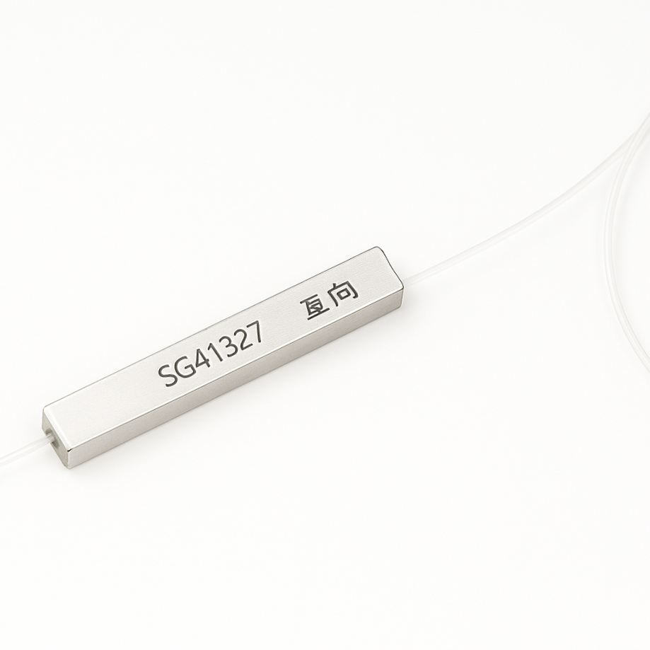
Spotlight: Scaling the PM Patchcord
Polarization-maintaining fibers represent a uniquely demanding challenge in optical manufacturing. Standard single-mode fibers are rotationally symmetrical. Polarization-maintaining fibers, however, are highly sensitive to orientation. This sensitivity makes them a prime case study for the difficulties encountered when scaling niche optical technologies.
The Complexity of Polarization-Maintaining Fibers
These specialized fibers are explicitly designed to maintain the polarization state of light. This characteristic is critical for gyroscopes, advanced sensors, and coherent communication networks. This stability is achieved through internal stress rods, typically in PANDA or Bow-tie configurations, that create birefringence within the glass.
When manufacturing a PM patchcord as custom fiber device, these microscopic stress rods must be precisely aligned with the mechanical key of the connector. Even a rotational error of just two degrees will cause cross-coupling between the fast and slow axes. This effectively destroys the optical integrity of the device.
Achieving High Extinction Ratios in Volume
The primary metric for quality in these devices is the Polarization Extinction Ratio. In a research lab, achieving a high Extinction Ratio exceeding 25dB or even 30dB involves painstaking manual rotation while staring at a polarimeter output. In volume production, this manual method is economically disastrous.
To solve this, advanced manufacturing facilities deploy automated active alignment systems. These sophisticated machines inject a polarized light source and continuously monitor the ratio in real-time. They utilize high-precision motorized rotary stages to lock the fiber axis into the exact optimal position before the epoxy is flashed. Furthermore, this automation ensures a low Insertion Loss strictly below 0.2dB across thousands of deployed units.
Mastering Optical-Electrical Integration in High-Volume Builds
Looking at the broader telecommunications and data center landscape, a clear industry trajectory is emerging. The aggressive push toward Co-Packaged Optics is reshaping hardware design. As switch bandwidths scale beyond 51.2 Tbps, traditional pluggable transceivers are hitting severe physical and thermal bottlenecks. Integrating silicon photonics directly alongside the switch ASIC is transitioning from a futuristic concept to a commercial necessity to curb massive power consumption.
The Demand for Miniaturization
The physical real estate available on server blades and network front panels is shrinking rapidly. This drives an intense demand for highly compact ultra-mini hybrid devices. Scaling these architectures means working with microscopic tolerances. Bare fiber arrays must be pitched perfectly to align with increasingly dense photodetector arrays. For example, maintaining a 127-micron pitch with sub-micron accuracy is now a standard requirement. The manufacturing process must account for handling these ultra-small form-factor components without causing micro-bends in the fiber or physical damage to the semiconductor dies.
Bridging Photonics and Electronics
The core challenge of optical-electrical integration lies in managing the conflicting physical needs of light and electricity simultaneously. Active electronic components, such as laser diodes and transimpedance amplifiers, generate substantial thermal loads.
When these components are densely packed alongside temperature-sensitive optical elements, thermal expansion can cause severe signal drift. Electromagnetic interference must also be heavily shielded. Scaling requires advanced packaging techniques where micro-heatsinks and precision optical alignments are manufactured concurrently within the same hybrid substrate.
Scalable Assembly for Hybrid Devices
Top-tier manufacturing partners handle this intricate integration by deploying multi-stage automated lines. These environments must seamlessly transition between photonics tasks, like active laser alignment, and electronics tasks, like printed circuit board mounting and reflow soldering. By utilizing automated dispensing systems that apply exact micro-volumes of thermal pastes and index-matching epoxies, manufacturers standardize this delicate integration. This precision is critical for maintaining profitable yields in volume hybrid production.
Quality Control and Testing Protocols for Mass Production
A working prototype does not guarantee a working production line. Assuming otherwise is a costly mistake. Stringent, scalable quality control protocols provide the only empirical data to guarantee field reliability.
Moving from Sample Testing to Inline Testing
During early pilot runs, manufacturers might rely on batch testing, checking perhaps one out of every ten units. For complex custom fiber builds, this is entirely insufficient. A single microscopic scratch on a fiber core or a slight epoxy void can render a device useless.
Therefore, scaling requires the implementation of continuous inline testing. Automated testing stations are built directly into the assembly flow. They evaluate every single unit for optical performance before it reaches the packaging phase. This immediate feedback loop prevents defective work-in-progress inventory from accumulating.
Key Optical Metrics to Monitor
Tracking performance at production speeds requires specialized testing rigs capable of rapid data acquisition. The following critical metrics must be monitored continuously:
Optical Metric | Definition & Importance | Automation Method in Volume Production |
|---|---|---|
Insertion Loss | The optical power lost when a signal passes through a device. Critical for maintaining tight network power budgets. | Automated multi-channel optical power meters integrated with robotic part handlers for rapid sequential testing. |
Return Loss | The ratio of reflected optical power back toward the source. High return loss prevents laser destabilization. | Optical Continuous Wave Reflectometry systems synchronized with inline testing stations. |
End-Face Geometry | The physical topography of the connector, including radius of curvature and apex offset. | Three-dimensional interferometry scanners that provide instant pass or fail data based on strict industry standards. |
Environmental and Stress Screening
Optical hardware deployed in telecommunications or industrial sectors must survive harsh real-world conditions for decades. Scalable quality control includes rigorous environmental screening based on established industry standards. This involves subjecting statistical samples from volume batches to accelerated aging. Units undergo aggressive thermal cycling, rapid shifts from extreme cold to extreme heat, damp heat exposure, and mechanical vibration testing. These stress screens verify that the materials chosen will maintain their structural and optical integrity over a twenty-year lifespan.
Cost Optimization Strategies for Custom Fiber Solutions
Scaling production is not merely an exercise in increasing output. It is equally about systematically driving down the cost per unit. Effective cost optimization requires a strategic approach to component selection and supply chain logistics.
Component Standardization
One of the most immediate ways to lower the bill of materials cost is through strategic component standardization. The core optical function of your device may be highly proprietary. However, the surrounding mechanical architecture often is not.
Engineering teams should identify areas where commercial off-the-shelf components can replace custom-tooled parts. Using standard strain relief boots, generic metal housings, or conventional jacketing for the non-critical sections of a build drastically reduces non-recurring engineering costs. This approach heavily leverages existing mass-production economies.
Yield Improvement as a Cost Saver
In the photonics industry, scrap rates are a massive driver of hidden costs. Throwing away a fully assembled, complex device because it failed final testing means wasting expensive raw materials and valuable labor hours.
Investing upfront in superior automated tooling and precise active alignment machines directly improves the first-pass yield. Drastically reducing scrap rates from thirty percent down to two percent is a far more sustainable method for lowering the overall cost per unit than simply haggling over the price of raw materials.
Strategic Supply Chain Management
Volume production requires a paradigm shift in procurement. Rather than purchasing materials on a sporadic, project-by-project basis, organizations must partner with a manufacturer that provides comprehensive Custom Fiber Solutions. An experienced partner possesses an established, vetted network of raw material suppliers. They can consolidate purchasing to secure volume discounts on specialty fibers and precision ferrules. Furthermore, they establish safety stock agreements that insulate your production line from volatile global supply chain disruptions.
Choosing the Right Manufacturing Partner for Your Build
The theoretical knowledge of how to scale is only as good as the facility executing the plan. Selecting a manufacturing partner is a critical business decision that ultimately dictates the success or failure of your product launch. You need actionable standards to evaluate potential partners.
Engineering and New Product Introduction Support
A common pitfall is contracting a manufacturer that operates strictly on a build-to-print basis. These facilities will build exactly what is on your drawing, even if the drawing contains inherent scaling flaws. A superior partner provides dedicated engineering support. Their internal optical engineers will actively collaborate with your team. They will audit the prototype, suggest crucial design improvements, and validate the assembly process before a single high-volume batch is initiated.
Advanced Facility Capabilities
Optical manufacturing demands highly controlled, pristine environments. Procurement teams must rigorously audit a potential partner physical infrastructure. Key requirements include certified cleanrooms, specifically Class 10,000 or better. This prevents microscopic dust from contaminating delicate optical interfaces during die bonding or splicing. The facility must be equipped with state-of-the-art machinery. Look for automated multi-axis polishing machines, laser welders for hermetic sealing, and automated optical inspection microscopes utilizing machine vision to detect microscopic end-face scratches.
Proven Track Record in Complex Builds
Experience is a non-transferable asset. A facility that excels at producing standard telecom patch cords may completely fail when tasked with scaling a highly sensitive polarization-maintaining device or a dense fiber array. A proven track record in handling specialized fibers, complex hybrid packaging, and custom form factors demonstrates a deep understanding of optical physics. This history provides empirical confidence that the manufacturer can navigate the strict tolerances of your specific build.
Conclusion
Scaling from a functional prototype to high-volume production is a multifaceted journey. It requires a fundamental shift in perspective. You must move away from pure conceptual innovation toward rigorous repeatability, process control, and cost efficiency. By embracing Design for Manufacturability early, investing in automated assembly, and implementing continuous inline testing, organizations can successfully navigate the transition from lab to line.
Whether you are deploying specialized polarization-maintaining sensors or pioneering new frontiers in hybrid co-packaged optics, the long-term success of your project hinges on robust manufacturing practices. Partnering with a facility that offers deep engineering support and advanced cleanroom capabilities will ultimately reduce your time to market. It ensures your optical innovations perform reliably in the field, exactly as designed.
Frequently Asked Questions
What is the biggest challenge when scaling custom optical builds?
The most significant challenge is maintaining exceptionally tight optical tolerances while simultaneously accelerating production throughput. In a lab setting, skilled engineers manually adjust a prototype to achieve optimal performance. Volume production relies on standardized processes. Transitioning from bespoke manual assembly to automated, repeatable manufacturing requires extensive redesigning, custom tooling, and rigorous process validation. This ensures minor variances do not compound into assembly line failures.
Why are polarization-maintaining devices difficult to manufacture in high volumes?
These fibers are inherently complex because they require exact rotational alignment of the internal stress rods to the mechanical key of the connector. Performing this alignment manually under a microscope is tedious and highly prone to human error. To manufacture these devices at scale while consistently maintaining a high Extinction Ratio, manufacturers must invest in automated active alignment stations. These systems dynamically rotate and lock the fiber into the perfect optical position.
How does integrating photonics with electronics impact the manufacturing process?
Hybrid integration significantly increases the complexity of the manufacturing environment. Traditional fiber optic assembly focuses primarily on mechanical alignment and cleanliness. Hybrid builds require managing precision optics and sensitive semiconductor electronics simultaneously. This necessitates specialized cleanroom environments, advanced thermal management solutions to dissipate heat from active components, and sophisticated automated equipment capable of handling bare fibers and circuitry without inducing mechanical stress.
How long does it take to scale from prototype to mass production in fiber optics?
The timeline varies heavily based on the complexity of the device, but it typically ranges from six to twelve months. This period includes the initial design audit, fabricating custom alignment fixtures, validating the automated assembly process, and conducting rigorous environmental stress testing. Rushing this phase often leads to catastrophic yield issues during the first high-volume run.
What is the typical yield rate for custom optical assemblies?
For highly complex, newly scaled optical devices, initial manual production runs might see yield rates as low as sixty percent. However, by implementing strict Design for Manufacturability principles, utilizing automated active alignment, and enforcing continuous inline testing, world-class manufacturers can push first-pass yield rates well above ninety-five percent. High yield is the most effective way to drive down the final cost per unit.
How can I reduce the cost of my custom fiber build without sacrificing quality?
The most effective strategy for cost reduction is implementing Design for Manufacturability principles early in the development cycle. By standardizing non-critical components, you reduce bill of material costs and eliminate unnecessary custom tooling fees. Designing the product for automated assembly rather than manual labor lowers ongoing operational costs. Investing in precise automated alignment improves your first-pass yield, drastically reducing scrap rates and lowering the true cost per unit at scale.
Ready to scale your next optical project? Whether you need ultra-miniature hybrid components or robust polarization-maintaining assemblies, finding the right manufacturing partner is your most critical step. Explore industry-leading, high-yield manufacturing capabilities tailored to your specific needs by visiting Kerns Tech to ensure your innovations transition seamlessly from the lab to global deployment.


